



 Audio 2G
Any digital source—whether it’s a streaming service, a NAS, a USB drive, or an S/PDIF input—is routed to Marantz’s proprietary processing platform. Analog sources, on the other hand, follow a completely different path, bypassing any analog-to-digital conversion and maintaining an entirely analog signal path all the way to the volume control section. This distinction is one of the most interesting aspects of the design. Many modern digital preamplifiers convert any analog source to digital to standardize its processing. Marantz, however, has chosen a different path, preserving the signal’s original character.
The MMM Converter, Marantz Musical Mastering
Unlike nearly all converters currently on the market, the LINK 10n does not use a commercial DAC chip manufactured by ESS, AKM, or Texas Instruments. The entire conversion process was developed in-house. The PCM signal, regardless of its original sampling frequency, is processed by a proprietary FPGA, where the first stage of the process—called MMM-Stream—takes place. Here, the PCM stream is completely reconstructed and converted into a one-bit DSD signal using a sophisticated sigma-delta modulator developed by Marantz. Next comes the second stage, MMM-Conversion, in which the DSD stream is converted directly to analog using a discrete one-bit converter followed by an analog low-pass filter. The result is an architecture that belongs neither to the family of R-2R converters nor to that of traditional delta-sigma DACs. Rather, it represents a modern reinterpretation of one-bit conversion, made possible by the computational power of contemporary FPGAs and the expertise Marantz has accumulated over more than thirty years of developing its own digital systems. Once the digital-to-analog conversion is complete, another fundamental element of the design comes into play: volume control. This is likely one of the least conspicuous yet most sophisticated aspects of the LINK 10n. Marantz has not disclosed the detailed operation of the circuit, but certain elements provide insight into its design philosophy. The presence of Source Direct mode and the absence of any mention of A/D conversions on the analog inputs suggest that analog sources follow a dedicated path, separate from the digital one. This means that the LINK 10n can be used as a true analog preamplifier without forcing the signal from a turntable or external player to undergo a double analog-to-digital and digital-to-analog conversion. Volume control thus represents the intersection between the sophisticated MMM platform and Marantz’s proprietary analog circuitry.
HDAM-3
Developed as an alternative to traditional integrated operational amplifiers, HDAMs use only carefully selected discrete components and have been one of the hallmarks of Marantz’s manufacturing for over thirty years; you can find a technical overview here. In the LINK 10n, they are used in the DAC’s output stage, the preamp section, the MM/MC phono circuit, and the headphone amplifier, creating a perfectly cohesive architecture. The electrical specifications confirm this design philosophy. The variable outputs feature extremely low impedance—30 ohms on the RCA connections and 140 ohms on the XLR connections—while the maximum available voltage reaches 10 and 20 volts RMS, respectively. These are values typically found in separate, very high-quality preamplifiers, allowing the LINK 10n to directly drive any power amplifier without difficulty.

Over-sized power supply
When you remove the top cover, you immediately see a design that is much more reminiscent of a high-end amplifier than that of a network streamer. The front panel houses two large toroidal transformers, which are completely separate and enclosed within dedicated shielding. The decision to use dual transformers stems not so much from the need to increase available power as from the desire to keep the power supplies for the digital and analog sections as independent as possible.
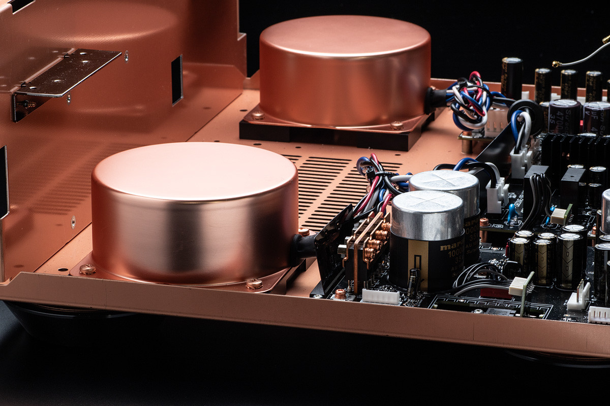
Downstream from the transformers, a dedicated circuit board handles rectification, initial filtering, and the distribution of current to the device’s various subsystems. Noteworthy is the presence of a sturdy copper busbar, a solution typical of high-power electronics and chosen to minimize resistance and inductance in the power path.
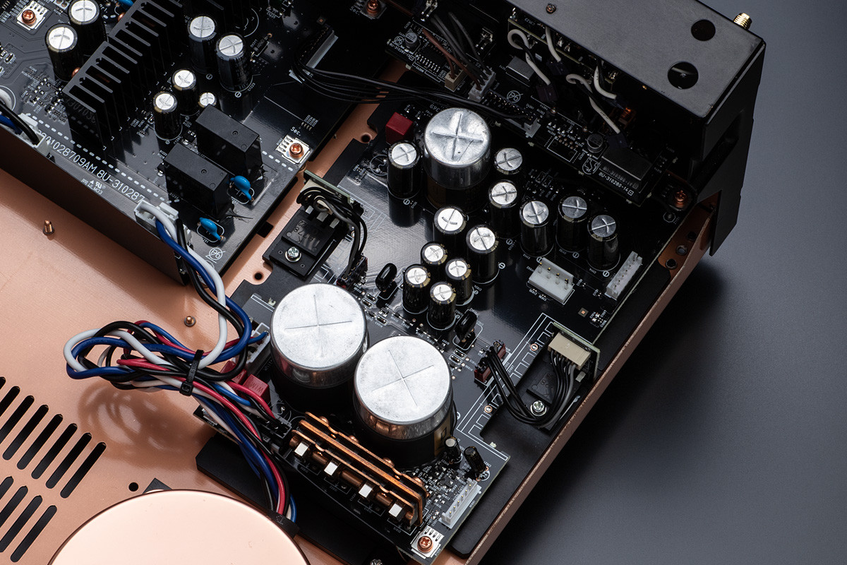
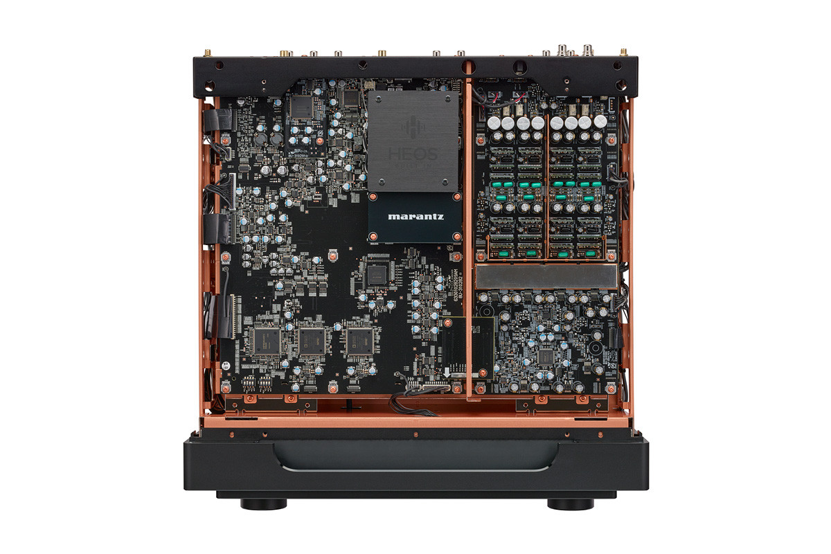
The filtering capability is not concentrated in a single central bank, but distributed near the various circuit sections. Each HDAM group has its own local decoupling, reducing the power supply impedance and ensuring an extremely fast response to current demands. The overall impression is that of a design developed starting from the power supply—and not ending with it. The internal layout also merits consideration. The interior photographs show a rigorous compartmentalization of the chassis. The power supply section occupies a dedicated area, completely separate from the HEOS and MMM digital platforms and the analog output stages. Each subsystem has its own physical space, minimizing the potential for mutual interference.




GIPHY App Key not set. Please check settings